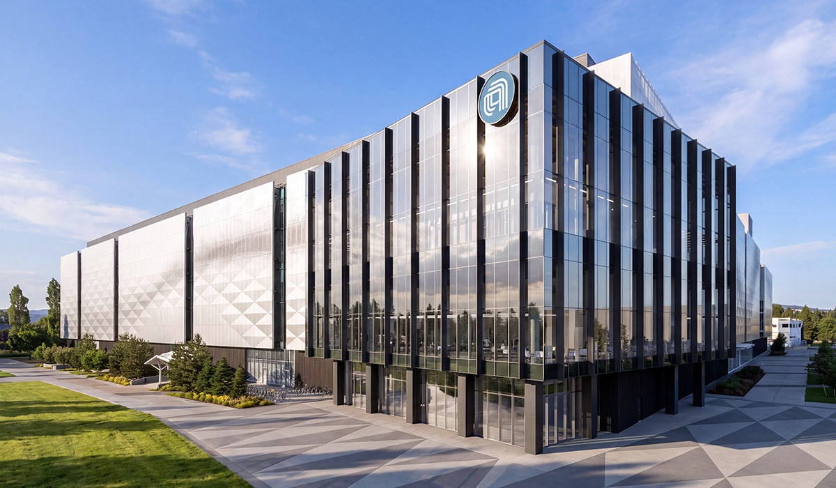
Facility tourapprovedOctober 12, 2026
Applied Materials
EPIC Center unveiling and partner open house
Applied Materials unveiled its completed EPIC Center in Sunnyvale, California, opening a 600,000-square-foot semiconductor equipment and process R&D facility to founding chipmakers, technology partners, and university researchers.
The October 12 unveiling moved Applied Materials' Equipment and Process Innovation and Commercialization Center from a multiyear construction project into an active collaboration site. The facility combines nearly four acres of advanced cleanroom space with teams from major chipmakers, equipment suppliers, systems companies, and universities, with the stated goal of shortening the path from materials research to manufacturing-ready semiconductor processes.
Headline metrics
| Capital investment | $5 billion | Applied Materials describes this as a capital investment that will scale over time as customer projects begin. |
| Facility area | 600,000 sq. ft. | Completed structure at Applied Materials' Sunnyvale campus. |
| Advanced cleanroom space | Nearly 4 acres | Company-reported cleanroom footprint inside the EPIC Center. |
| Construction effort | More than 6 million hours | Company-reported construction hours required to complete the center. |
Highlights
- Completed and openedApplied Materials said construction was complete and that the center opened with an initial roster of industry and research partners.
- Founding chipmakersTSMC, Intel, SK hynix, Micron, and Samsung Electronics are listed as founding partners.
- Manufacturing-relevant R&DThe center colocates materials research, equipment and process development, process integration, and pilot-production work.
Resources
- Applied Materials press releaseappliedmaterials.com